
Product laser
Products
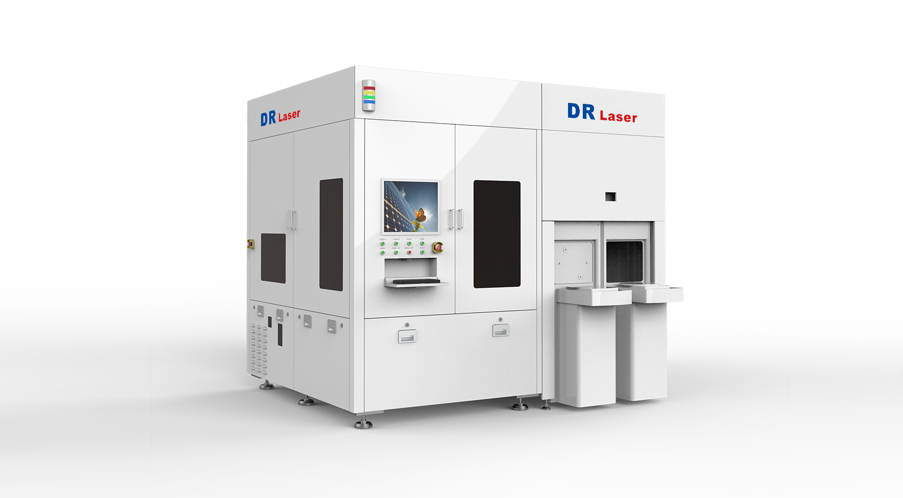
Activation depth ≥ 7 μm
Throughput > 25 wafers per hour @ 8-inch
Excellent sheet resistance uniformity and surface appearance
Full-process in-situ monitoring and feedback capability
Supports ultra-thin wafers, TAIKO wafers, and warped wafers
Equipped with laser-assisted heating system
| Specification | DR-S-LA200S | DR-S-LA300S | DR-S-LA200D | DR-S-LA300D |
| Compatible Wafer Sizes | 6"/8" compatible | 8"/12" compatible | 6"/8" compatible | 8"/12" compatible |
| Laser Energy Density | ≥ 5 J/cm2 | ≥ 5 J/cm2 | ≥ 5 J/cm2 | ≥ 5 J/cm2 |
| Laser Stability | ≤ 2%, RMS | |||
| Activation Rate | ≥ 95% @B Implant, ≥ 90% @P Implant | |||
| Uniformity | Intra-wafer: ≤ 1%, Inter-wafer: ≤ 1% @ 8", RS | |||
| Cleanliness Control | ≤ 30 @ 0.5 μm, ≤ 5 @ 1 μm | |||
| Automation System | Dual wafer loading ports, multi-axis robotic arm, pre-alignment unit | |||